Thursday 27 December 2012

PROGRAMMABLE INTERRUPT CONTROLLER - INTEL 8259


FEATURES OF 8259:


1. It is programmed to work with either 8085 or 8086 processor.


2. It manage 8-interrupts according to the instructions written into its control registers.


3. In 8086 processor, it supplies the type number of the interrupt and the type number is programmable. In 8085 processor, the interrupt vector address is programmable. The priorities of the interrupts are programmable.


4. The interrupts can be masked or unmasked individually.


5. The 8259s can be cascaded to accept a maximum of 64 interrupts.

Water level Controller

The water level Controller is a reliable circuit, it takes over the task of indicating and Controlling the water level in the overhead water tanks. The level of the water is displayed in the LED Bar graph. The Copper probes are used to sense the water level. The probes are inserted into the water tank which is to be monitored. This water-level Controller-cum-alarm circuit is configured around the well-known 8 bit Microprocessor 8085. It continuously monitors the overhead water level and display it and it also switch Off the Motor when the tank fills and it will automatically switch On the Motor when the water level is low. The Microprocessor will also indicate the water level over the LED display. All the input and output functions are done through the Programmable Peripheral Interface IC 8255.

Monday 24 December 2012

LCD based digital alarm clock

An alarm clock is a clock that indicates a pre-set time by producing sound at that time. This functionality of digital clock is used to awaken people or remind them of something. This circuit is an extension to the digital clock with time setting option. Here an extra switch is provided to set the alarm. While the alarm is set, the clock time does not stop and runs in the background.The circuit is build around 8051 micro-controller (AT89C51) and uses LCD to display time.

Sunday 23 December 2012

Celsius and fahrenheit scale digital thermometer using AT89C51

Fahrenheit scale digital thermometer is a temperature indicator which displays temperature in Fahrenheit scale. It is similar to Celsius scale digital thermometer, except a little modification in the microcontroller program. The temperature sensed in Celsius scale in the Celsius scale thermometer project is converted into the Fahrenheit scale temperature just by using the Celsius to Fahrenheit conversion formulae. This project also uses 8051 microcontroller (AT89C51).

Saturday 22 December 2012

Simple Digital clock using 8051 microcontroller (AT89C51)

A digital clock is one that displays time digitally. The circuit explained here displays time with two ‘minutes’ digits and two ‘seconds’ digits on four seven segment displays. The seven segment and switches are interfaced with 8051 microcontroller AT89C51. This circuit can be used in cars, houses, offices etc.

Automatic bidirectional visitor counter using 8051 microcontroller (AT89C51)


A counter that can change its state in either direction, under control of an up–down selector input, is known as an up–down counter. The circuit given here can count numbers from 0 to 9999 in up and down modes depending upon the state of the selector. It can be used to count the number of persons entering a hall in the up mode at entrance gate. In the down mode, it can count the number of persons leaving the hall by decrementing the count at exit gate. It can also be used at gates of parking areas and other public places.
This circuit divided in three parts: sensor, controller and counter display. The sensor would observe an interruption and provide an input to the controller which would run the counter in up/down mode depending upon the selector setting. The same count is displayed on a set of 7-segment displays through the controller.

Monday 26 November 2012

interface 16x2 LCD with 8051 microcontroller


Interface a keypad with Microcontroller

Keypad is a widely used input device with lots of application in our everyday life. From a simple telephone to keyboard of a computer, ATM, electronic lock, etc., keypad is used to take input from the user for further processing. In this article we are interfacing keypad with the MCU AT89C51 and displaying the corresponding number on LCD. This module can be further used in a number of systems to interfaced keypad with microcontroller and other processors to get desired output.


Keypad is organized as a matrix of switches in rows and column. The article uses a 4X3 matrix keypad and a 16x2 LCD for displaying the output of keypad.
The circuit diagram shows the connection of keypad with the controller. Port P2 of the microcontroller is used to send the data for displaying on the LCD. P1^1, P1^2, P1^3 pins of microcontroller is connected to RS, RW, EN pins of LCD respectively. Port P0 is used to scan input from the keypad (refer circuit diagram for connection).

The concept of interfacing keypad with the MCU is simple. Every number is assigned two unique parameters, i.e., row and column number (n(R, C) for example 6 (2, 3)). Hence every time a key is pressed the number is identified by detecting the row and column number of the key pressed.

Initially all the rows are set to zero by the controller and the columns are scanned to check if any key is pressed. In case no key is pressed the output of all the columns will be high.

Saturday 24 November 2012

Internal block diagram of DACO800


  • The DAC0800 is an 8-bit, high speed, current output DAC with a typical settling time (conversion time) of 100 ns.


  • It produces complementary current output, which can be converted to voltage by using simple resistor load.


  • The DAC0800 require a positive and a negative supply voltage in the range of ± 5V to ±18V.


  • It can be directly interfaced with TTL, CMOS, PMOS and other logic families.


  • For TTL input, the threshold pin should be tied to ground (VLC = 0V).


  • The reference voltage and the digital input will decide the analog output current, which can be converted to a voltage by simply connecting a resistor to output terminal or by using an op-amp I to V converter.


  • The DAC0800 is available as a 16-pin IC in DIP

Interfacing of 4x4 matrix keyboard and 4 digit 7 segment display

  • 4 scan lines are sufficient to scan matrix keyboard and to select display digits. Hence decoded mode is used.

Thursday 25 October 2012

8257 DMA CONROLLER

  • The Intel 8257 is a programmable, 4-channel DMA controller (DMAC)
  • 4 peripherals can request data transfer simultanously
  • It is a 40-pin DIP IC


PINOUT DIAGRAM OF 8255 PPI


Intel 8255 (or i8255) Programmable Peripheral Interface


  • The Intel 8255 is an intelligent programmable peripheral interface (PPI)ii
  • It is a multiport input/output device
  • It is a general purpose device for interfacing parallel I/O device to microprocessor/microcontroller bus
  • Some manufactures use the term 'peripheral interface adapter'
  • The main function of 8255 PPI ae to interface peripheral devices to microcomputer system
  • It is a 40-pin DIP IC
  • It operated on a single +5v dc supply
  • It gas three 8-bit I/O ports, namely, Port A, Port B, & Port C
  • Port C is further divided into two 4-bit ports-Port C upper & Port C lower
  • Total 4-Ports are available, two 8-bit ports & two 4-bit Ports 
  • Each port can be programmed as an input port or an output port 
  • It has an 8-bit internal register to store the control word. the control word is used to configure the three ports of 8255 either as input or as output


FEATURES OF MICROCONTOLLERS

  • As all the peripherals are integrated into a single chip, the overall system cost is very low
  • The product is of a small size as compared to the microprocessor based systems and is thus very handy
  • The system design requires very little efforts and is easy to trouble shoot and maintain 
  • As the peripheral are integrated with a mp, the system is more reliable
  • Though a microcontroller have on-chip RAM,ROM & I/O ports, additional RAM,ROM,I/O ports may be interfaced externally if required
  • The microcontrollers with on-chip ROM provides a software security feature which is not available with microprocessor based systems using ROM/EPROM
  • All these features are available in a 40-pin packages as in 8-bit processor


Wednesday 24 October 2012

COMPLEX INSTRUCTION SET COMPUTER (CISC)

  • A complex instruction set computer  is a computer where single instructions can execute several low-level operations (such as a load from memory, an arithmetic operation, and a memory store) and/or are capable of multi-step operations or addressing modes within single instructions
  • Generally, the instruction set of a CISC system is made efficient by incorporating a large number of powerful instructions
  • Instructions are executed by micro-program
  • Variable format instructions
  • Supports complex addressing mode
  • CISC systems have following drawbacks:
  1. CPU COMPLEXITY : The control unit design (mainly instruction decoding) becomes complex since the instruction set is large with heavily encoded instructions
  2. SYSTEM SIZE & COST: There is a lot of hardware circuitry due to complexity of the CPU. This increases the hardware cost of the system and also the power requirements
  3. CLOCK SPEED: due to increase circuits the propagation delays are more and the CPU cycle time is large & hence the effective clock speed is reduced
  4. RELIABILITY: The heavy hardware is prone to frequent failures
  5. MAINTAINABILITY: Troubleshooting & detecting a fault is a big task since there are a large number of huge circuits. The invention  of microprogramming has reduced this burden to some extent. In built diagnostic microcodes were also provided in many CISC systems giving a helping hand to the hardware engineer in case of system failure.

Tuesday 23 October 2012

INTEL 80486 (i486)


  • The 80486 is the CPU with an on-chip floating point unit, introduced in 1989
  • It is advanced, evolutionary high performance 32-bit microprocessor 
  • It is fabricated using CHMOS -IV technology
  •  It is a CISC (complex instruction set computer) processor
  • It has 32-bit data bus
  • It has 32-bit address bus
  • It is available in 168-pin PGA (pin grid array) package
  • It contains more than 1.2 million transistors 
  • It is currently available with 25MHz , 33MHz, 50MHz, 66MHz & 100MHz clock
  • It contains 8KB cache & an arithmetic coprocessor
  • It executes many instructions in one clock period 

Monday 22 October 2012

MEMORY ORGANISATION OF 8086

Program, data and stack memories occupy the same memory space. The total addressable memory size is 1MB KB. As the most of the processor instructions use 16-bit pointers the processor can effectively address only 64 KB of memory. To access memory outside of 64 KB the CPU uses special segment registers to specify where the code, stack and data 64 KB segments are positioned within 1 MB of memory (see the "Registers" section below).

16-bit pointers and data are stored as:
address: low-order byte
address+1: high-order byte


32-bit addresses are stored in "segment:offset" format as:
address: low-order byte of segment
address+1: high-order byte of segment
address+2: low-order byte of offset
address+3: high-order byte of offset

Physical memory address pointed by segment:offset pair is calculated as:

address = (<segment> * 16) + <offset>

Program memory - program can be located anywhere in memory. Jump and call instructions can be used for short jumps within currently selected 64 KB code segment, as well as for far jumps anywhere within 1 MB of memory. All conditional jump instructions can be used to jump within approximately +127 - -127 bytes from current instruction.

Data memory - the 8086 processor can access data in any one out of 4 available segments, which limits the size of accessible memory to 256 KB (if all four segments point to different 64 KB blocks). Accessing data from the Data, Code, Stack or Extra segments can be usually done by prefixing instructions with the DS:, CS:, SS: or ES: (some registers and instructions by default may use the ES or SS segments instead of DS segment).

Word data can be located at odd or even byte boundaries. The processor uses two memory accesses to read 16-bit word located at odd byte boundaries. Reading word data from even byte boundaries requires only one memory access.

Stack memory can be placed anywhere in memory. The stack can be located at odd memory addresses, but it is not recommended for performance reasons (see "Data Memory" above).

Reserved locations:0000h - 03FFh are reserved for interrupt vectors. Each interrupt vector is a 32-bit pointer in format segment:offset.
FFFF0h - FFFFFh - after RESET the processor always starts program execution at the FFFF0h address

FLAG REGISTER OF 8086

Flags is a 16-bit register containing 9 1-bit flags:
  • Overflow Flag (OF) - set if the result is too large positive number, or is too small negative number to fit into destination operand.
  • Direction Flag (DF) - if set then string manipulation instructions will auto-decrement index registers. If cleared then the index registers will be auto-incremented.
  • Interrupt-enable Flag (IF) - setting this bit enables maskable interrupts.
  • Single-step Flag (TF) - if set then single-step interrupt will occur after the next instruction.
  • Sign Flag (SF) - set if the most significant bit of the result is set.
  • Zero Flag (ZF) - set if the result is zero.
  • Auxiliary carry Flag (AF) - set if there was a carry from or borrow to bits 0-3 in the AL register.
  • Parity Flag (PF) - set if parity (the number of "1" bits) in the low-order byte of the result is even.
  • Carry Flag (CF) - set if there was a carry from or borrow to the most significant bit during last result calculation.

ADDRESSING MODES OF 8086


Implied - the data value/data address is implicitly associated with the instruction.

Register - references the data in a register or in a register pair.

Immediate - the data is provided in the instruction.

Direct - the instruction operand specifies the memory address where data is located.

Register indirect - instruction specifies a register containing an address, where data is located. This addressing mode works with SI, DI, BX and BP registers.

Based - 8-bit or 16-bit instruction operand is added to the contents of a base register (BX or BP), the resulting value is a pointer to location where data resides.

Indexed - 8-bit or 16-bit instruction operand is added to the contents of an index register (SI or DI), the resulting value is a pointer to location where data resides.

Based Indexed - the contents of a base register (BX or BP) is added to the contents of an index register (SI or DI), the resulting value is a pointer to location where data resides.

Based Indexed with displacement - 8-bit or 16-bit instruction operand is added to the contents of a base register (BX or BP) and index register (SI or DI), the resulting value is a pointer to location where data resides.

REGISTER ORGANISATION OF 8086


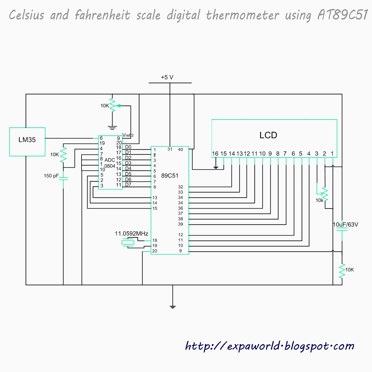
Most of the registers contain data/instruction offsets within 64 KB memory segment. There are four different 64 KB segments for instructions, stack, data and extra data. To specify where in 1 MB of processor memory these 4 segments are located the 8086 microprocessor uses four segment registers:

Code segment (CS) is a 16-bit register containing address of 64 KB segment with processor instructions. The processor uses CS segment for all accesses to instructions referenced by instruction pointer (IP) register. CS register cannot be changed directly. The CS register is automatically updated during far jump, far call and far return instructions.

Stack segment (SS) is a 16-bit register containing address of 64KB segment with program stack. By default, the processor assumes that all data referenced by the stack pointer (SP) and base pointer (BP) registers is located in the stack segment. SS register can be changed directly using POP instruction.

Data segment (DS) is a 16-bit register containing address of 64KB segment with program data. By default, the processor assumes that all data referenced by general registers (AX, BX, CX, DX) and index register (SI, DI) is located in the data segment. DS register can be changed directly using POP and LDS instructions.

Extra segment (ES) is a 16-bit register containing address of 64KB segment, usually with program data. By default, the processor assumes that the DI register references the ES segment in string manipulation instructions. ES register can be changed directly using POP and LES instructions.

It is possible to change default segments used by general and index registers by prefixing instructions with a CS, SS, DS or ES prefix.

All general registers of the 8086 microprocessor can be used for arithmetic and logic operations. The general registers are:

Accumulator register consists of 2 8-bit registers AL and AH, which can be combined together and used as a 16-bit register AX. AL in this case contains the low-order byte of the word, and AH contains the high-order byte. Accumulator can be used for I/O operations and string manipulation.

Base register consists of 2 8-bit registers BL and BH, which can be combined together and used as a 16-bit register BX. BL in this case contains the low-order byte of the word, and BH contains the high-order byte. BX register usually contains a data pointer used for based, based indexed or register indirect addressing.

Count register consists of 2 8-bit registers CL and CH, which can be combined together and used as a 16-bit register CX. When combined, CL register contains the low-order byte of the word, and CH contains the high-order byte. Count register can be used as a counter in string manipulation and shift/rotate instructions.

Data register consists of 2 8-bit registers DL and DH, which can be combined together and used as a 16-bit register DX. When combined, DL register contains the low-order byte of the word, and DH contains the high-order byte. Data register can be used as a port number in I/O operations. In integer 32-bit multiply and divide instruction the DX register contains high-order word of the initial or resulting number.

The following registers are both general and index registers:

Stack Pointer (SP) is a 16-bit register pointing to program stack.

Base Pointer (BP) is a 16-bit register pointing to data in stack segment. BP register is usually used for based, based indexed or register indirect addressing.

Source Index (SI) is a 16-bit register. SI is used for indexed, based indexed and register indirect addressing, as well as a source data address in string manipulation instructions.

Destination Index (DI) is a 16-bit register. DI is used for indexed, based indexed and register indirect addressing, as well as a destination data address in string manipulation instructions.

PINOUT DIAGRAM OF 8086


INTEL 80386


  • The intel 80386 is the 1st 32-bit microprocessor introduced in 1985
  • It is a logical extension of 8086 & 80286
  • It has 32-bit data bus & 32 bit internal registers
  • 32-bit ALU
  • It is a 132 pin IC available in PGA (Pin Grid Array) package
  • It uses a single +5v DC for the operation
  • It has 32-bit non-muxed address bus
  • It has break point registers
  • It is capable of addressing 4 GB of Physical memory & 64 TB of virtual memory
  • It is fabricated using CHMOS-III technology
  • I contains 129 basic instructions
  • It is software object code compatible with 8086 & 80286
  • It contains 275,000 transistors on a single chip

Sunday 21 October 2012

INTEL 80286


  • The intel 80286 microprocessor is an advanced version of the 8086 microprocessor that was designed , for multipurpose , multi-tasking,multi user enviroments in 1983
  • The 80286 is a high performance, 16-bit microprocessor with on-chip memory protection & management capabilities
  • It finds its applications in control systems as an embedded controller
  • It is available in 68-pin PLCC (plastic lead chip carrier), 68-pin LCC(Leadless Chip Carrier)& 68-pin PGA (Pin Grid Array) packages
  • It has 24 address lines
  • It address 16 MB of physical memory  & 1GB of virtual memory
  • The 80286 works in 2 operating modes - Real Address Mode (RAM) & protected virtual address made (PVAM). The operation of RAM is objected compatible & PVAM is source code compatible
  • It is 6 times faster than the 8086
  • The internal structure of 80286 contains 4 separate processing units. these are Bus Interface Unit (BIU), Instruction Unit (IU), Address Unit (AU) & Execution Unit (EU)
  • The 80286 does not contains a muxed address/data bus
  • I prevents the applications programs from performing I/O responding to interrupts & calling the system service directly excepted through pre-established entry points.

INTEL 8086


  • Intel 8086 is a 1st member of 80x86 microprocessor family
  • It is a 16-bit microprocessor
  • It supports 16-bit ALU
  • A set of 16-bit registers
  • Most of the instructions are designed to work with 16-bit binary words
  • It has 16-bit data bus
  • It can be data from or write data into memory & ports either 8-bit or 16-bit at a time
  • It has 20-bit address lines so it can address 220 =1,048,576 (1mb) memory locations
  • It provide segment memory addressing capability
  • A rich instruction set
  • Powerful interrupt structure 
  • 6 byte instruction queue
  • Max clock frequency is 5,8,10MHz
  • Memory divided into 2 banks (even & odd)
  • Address range of memory is 00000-FFFFFH

Sunday 7 October 2012

PINOUT OF 8051


Pins 1-8: Port 1 Each of these pins can be configured as an input or an output.

Pin 9: RS A logic one on this pin disables the microcontroller and clears the contents of most registers. In other words, the positive voltage on this pin resets the microcontroller. By applying logic zero to this pin, the program starts execution from the beginning.

Pins10-17: Port 3 Similar to port 1, each of these pins can serve as general input or output. Besides, all of them have alternative functions:

Pin 10: RXD Serial asynchronous communication input or Serial synchronous communication output.

Pin 11: TXD Serial asynchronous communication output or Serial synchronous communication clock output.

Pin 12: INT0 Interrupt 0 input.

Pin 13: INT1 Interrupt 1 input.

Pin 14: T0 Counter 0 clock input.

Pin 15: T1 Counter 1 clock input.

Pin 16: WR Write to external (additional) RAM.

Pin 17: RD Read from external RAM.

Pin 18, 19: X2, X1 Internal oscillator input and output. A quartz crystal which specifies operating frequency is usually connected to these pins. Instead of it, miniature ceramics resonators can also be used for frequency stability. Later versions of microcontrollers operate at a frequency of 0 Hz up to over 50 Hz.

Pin 20: GND Ground.

Pin 21-28: Port 2 If there is no intention to use external memory then these port pins are configured as general inputs/outputs. In case external memory is used, the higher address byte, i.e. addresses A8-A15 will appear on this port. Even though memory with capacity of 64Kb is not used, which means that not all eight port bits are used for its addressing, the rest of them are not available as inputs/outputs.

Pin 29: PSEN If external ROM is used for storing program then a logic zero (0) appears on it every time the microcontroller reads a byte from memory.

Pin 30: ALE Prior to reading from external memory, the microcontroller puts the lower address byte (A0-A7) on P0 and activates the ALE output. After receiving signal from the ALE pin, the external register (usually 74HCT373 or 74HCT375 add-on chip) memorizes the state of P0 and uses it as a memory chip address. Immediately after that, the ALU pin is returned its previous logic state and P0 is now used as a Data Bus. As seen, port data multiplexing is performed by means of only one additional (and cheap) integrated circuit. In other words, this port is used for both data and address transmission.

Pin 31: EA By applying logic zero to this pin, P2 and P3 are used for data and address transmission with no regard to whether there is internal memory or not. It means that even there is a program written to the microcontroller, it will not be executed. Instead, the program written to external ROM will be executed. By applying logic one to the EA pin, the microcontroller will use both memories, first internal then external (if exists).

Pin 32-39: Port 0 Similar to P2, if external memory is not used, these pins can be used as general inputs/outputs. Otherwise, P0 is configured as address output (A0-A7) when the ALE pin is driven high (1) or as data output (Data Bus) when the ALE pin is driven low (0).

Pin 40: VCC +5V power supply.

INTEL 8051 MICRO-CONTROLLER


  • The intel 8051 is an 8-bit micocontroller with 128 byte internal RAM & 4kb internal ROM.
  • 8051 is a 40 pin DIP IC 
  • It require +5v power supply
  • max clock frequency rating is 12MHz
  • It has 32 I/O ports & They are organised as 4 number of 8-bit parallel port
  • It has harvard architecture in which the same address in different memory device or bank is used for program & data
  • The architecture has two dedicated 16-bit pointers namely program counter (pc) & Data Pointer (DPTR)
  • The PC is used as address pointer to access program instructions & it is automatically incremented after every byte of instruction fetch
  • The DPTR is used as address pointer to read/write data in data memory & it is programmable using instructions 
  • It has 16-bit address bus & 8-bit data bus
  • They can address upto 64 k memory locations
  • it supports 2 memory banks of 64kb each one for program & other for data
  • It ha a separate 256 bytes internal RAM accessed by using 8-bit address 

MICRO CONTROLLER


  • The micro-controller similar to microprocessors, But they are designed to work as a true single chip system by integrating all the devices needed for a system on a chip
  • The basic functional units of a mp will be ALU, a set of registers,timing & control unit. the basic micro-controller will have these functional blocks & in addition may have I/O ports,programmable timer,RAM memory & EPROM/EEPROM memory
  • The micro-controller is concerned with rapid movement of code & data within microcontroller: hence it has few instruction for data transfer between external memory & micro-controller
  • The mc often manipulate with bits & so has large number of bit manipulating instruction 
  • The mc can be used to form a single chip microcomputer based system without any additional ICs
  • MC are used for designing application specific dedicated systems

Thursday 4 October 2012

ADSP 21XXX SHARC


  • High performance superharvard architecture
  • 32-bit processor
  • It can execute every instruction in a single cycle
  • Fast,flexible arithmetical computation units
  • Dual address generators
  • Efficient program sequencing
  • It has 10-port data register file
  • The ADSP 21000 family processors have 2 data address generators
  • Architectural features supporting high level languages and operating systems 
  • support IEEE 1149,IJTAG serial scan path & on-chip emulation features
  • General purpose data & address register file
  • Large address space 
  • Pre & post modify addressing
  • Onchip program , loop & interrupt stacks   

TMS 320C4X DIGITAL SIGNAL PROCESSOR


  • Highest performance floating point digital signal processor
  • It has 6 communication ports
  • 6 channel DMA coprocessor
  • Single cycle 40-bit floating point,32-bit integer multiplier
  • 40 bit reegisters,8 auxiliary registers
  • 14 control registers
  • 2 timers
  • 5v operation
  • Separate internal program,data & DMA coprocessor buses for support of massive concurrent input/output of program and data through put, maximizing sustained cpu performance
  • The c4x cpu has a register based architecture

Saturday 22 September 2012

Pin details of 8085

  • Pin Description
The following describes the function of each pin:


  • A6 - A1s (Output 3 State)
Address Bus; The most significant 8 bits of the memory address or the 8 bits of the I/0 address,3 stated during Hold and Halt modes.


  • AD0 - 7 (Input/Output 3state)
Multiplexed Address/Data Bus; Lower 8 bits of the memory address (or I/0 address) appear on the bus during the first clock cycle of a machine state. It then becomes the data bus during the second and third clock cycles. 3 stated during Hold and Halt modes.


  • ALE (Output)
Address Latch Enable: It occurs during the first clock cycle of a machine state and enables the address to get latched into the on chip latch of peripherals. The falling edge of ALE is set to guarantee setup and hold times for the address information. ALE can also be used to strobe the status information. ALE is never 3stated.


  • SO, S1 (Output)
Data Bus Status. Encoded status of the bus cycle:
S1 S0
O O HALT
0 1 WRITE
1 0 READ
1 1 FETCH
S1 can be used as an advanced R/W status.

  • RD (Output 3state)
READ; indicates the selected memory or 1/0 device is to be read and that the Data Bus is available for the data transfer.


  • WR (Output 3state)
WRITE; indicates the data on the Data Bus is to be written into the selected memory or 1/0 location. Data is set up at the trailing edge of WR. 3stated during Hold and Halt modes.


  • READY (Input)
If Ready is high during a read or write cycle, it indicates that the memory or peripheral is ready to send or receive data. If Ready is low, the CPU will wait for Ready to go high before completing the read or write cycle.


  • HOLD (Input)
HOLD; indicates that another Master is requesting the use of the Address and Data Buses. The CPU, upon receiving the Hold request. will relinquish the use of buses as soon as the completion of the current machine cycle. Internal processing can continue.
The processor can regain the buses only after the Hold is removed. When the Hold is acknowledged, the Address, Data, RD, WR, and IO/M lines are 3stated.

  • HLDA (Output)
HOLD ACKNOWLEDGE; indicates that the CPU has received the Hold request and that it will relinquish the buses in the next clock cycle. HLDA goes low after the Hold request is removed. The CPU takes the buses one half clock cycle after HLDA goes low.


  • INTR (Input)
INTERRUPT REQUEST; is used as a general purpose interrupt. It is sampled only during the next to the last clock cycle of the instruction. If it is active, the Program Counter (PC) will be inhibited from incrementing and an INTA will be issued. During this cycle a RESTART or CALL instruction can be inserted to jump to the interrupt service routine. The INTR is enabled and disabled by software. It is disabled by Reset and immediately after an interrupt is accepted.


  • INTA (Output)
INTERRUPT ACKNOWLEDGE; is used instead of (and has the same timing as) RD during the Instruction cycle after an INTR is accepted. It can be used to activate the 8259 Interrupt chip or some other interrupt port.
RST 5.5
RST 6.5 - (Inputs)
RST 7.5
  • RESTART INTERRUPTS; These three inputs have the same timing as I NTR except they cause an internal RESTART to be automatically inserted.
RST 7.5 ~~ Highest Priority
RST 6.5
RST 5.5 o Lowest Priority
The priority of these interrupts is ordered as shown above. These interrupts have a higher priority than the INTR.


  • TRAP (Input)
Trap interrupt is a nonmaskable restart interrupt. It is recognized at the same time as INTR. It is unaffected by any mask or Interrupt Enable. It has the highest priority of any interrupt.


  • RESET IN (Input)
Reset sets the Program Counter to zero and resets the Interrupt Enable and HLDA flipflops. None of the other flags or registers (except the instruction register) are affected The CPU is held in the reset condition as long as Reset is applied.


  • RESET OUT (Output)
Indicates CPlJ is being reset. Can be used as a system RESET. The signal is synchronized to the processor clock.


  • X1, X2 (Input)
Crystal or R/C network connections to set the internal clock generator X1 can also be an external clock input instead of a crystal. The input frequency is divided by 2 to give the internal operating frequency.


  • CLK (Output)
Clock Output for use as a system clock when a crystal or R/ C network is used as an input to the CPU. The period of CLK is twice the X1, X2 input period.


  • IO/M (Output)
IO/M indicates whether the Read/Write is to memory or l/O Tristated during Hold and Halt modes.


  • SID (Input)
Serial input data line The data on this line is loaded into accumulator bit 7 whenever a RIM instruction is executed.


  • SOD (output)
Serial output data line. The output SOD is set or reset as specified by the SIM instruction.


  • Vcc
+5 volt supply.


  • Vss
Ground Reference.

Flag Register Of 8085


Friday 21 September 2012

Pin-out diagram of 8085


Interrupts in 8085


The 8085 microprocessor has 5 interrupts. They are presented below in the order of their priority (from lowest to highest):
INTR is maskable 8080A compatible interrupt. When the interrupt occurs the processor fetches from the bus one instruction, usually one of these instructions:
  • One of the 8 RST instructions (RST0 - RST7). The processor saves current program counter into stack and branches to memory location N * 8 (where N is a 3-bit number from 0 to 7 supplied with the RST instruction).
  • CALL instruction (3 byte instruction). The processor calls the subroutine, address of which is specified in the second and third bytes of the instruction.
RST5.5 is a maskable interrupt. When this interrupt is received the processor saves the contents of the PC register into stack and branches to 2Ch (hexadecimal) address.
RST6.5 is a maskable interrupt. When this interrupt is received the processor saves the contents of the PC register into stack and branches to 34h (hexadecimal) address.
RST7.5 is a maskable interrupt. When this interrupt is received the processor saves the contents of the PC register into stack and branches to 3Ch (hexadecimal) address.
Trap is a non-maskable interrupt. When this interrupt is received the processor saves the contents of the PC register into stack and branches to 24h (hexadecimal) address.
All maskable interrupts can be enabled or disabled using EI and DI instructions. RST 5.5, RST6.5 and RST7.5 interrupts can be enabled or disabled individually using SIM instruction.

Intel 8085 microprocessor & Architecture


  • The Intel 8085 is an 8-bit microprocessor introduced by Intel in 1977 
  • Max. CPU clock rate 3, 5 and 6 MHz 
  • The "5" in the model number came from the fact that the 8085 requires only a +5-volt (V) power supply 
  • The 8085 is a conventional von Neumann design based on the Intel 8080 
  • It has 8-bit data bus & 16-bit address bus 
  • The 8-bit data bus was instead multiplexed with the lower part of the 16-bit address bus to limit the number of pins to 40 
  • The 8085 has extensions to support new interrupts, with three maskable interrupts (RST 7.5, RST 6.5 and RST 5.5) 


Instruction set of 8080


8080 instruction set consists of the following instructions:
  • Data moving instructions.
  • Arithmetic - add, subtract, increment and decrement.
  • Logic - AND, OR, XOR and rotate.
  • Control transfer - conditional, unconditional, call subroutine, return from subroutine and restarts.
  • Input/Output instructions.
  • Other - setting/clearing flag bits, enabling/disabling interrupts, stack operations, etc.

REGISTER ORGANISATION OF 8080


Accumulator or A register is an 8-bit register used for arithmetic, logic, I/O and load/store operations.
Flag is an 8-bit register containing 5 1-bit flags:
  • Sign - set if the most significant bit of the result is set.
  • Zero - set if the result is zero.
  • Auxiliary carry - set if there was a carry out from bit 3 to bit 4 of the result.
  • Parity - set if the parity (the number of set bits in the result) is even.
  • Carry - set if there was a carry during addition, or borrow during subtraction/comparison.
General registers:
  • 8-bit B and 8-bit C registers can be used as one 16-bit BC register pair. When used as a pair the C register contains low-order byte. Some instructions may use BC register as a data pointer.
  • 8-bit D and 8-bit E registers can be used as one 16-bit DE register pair. When used as a pair the E register contains low-order byte. Some instructions may use DE register as a data pointer.
  • 8-bit H and 8-bit L registers can be used as one 16-bit HL register pair. When used as a pair the L register contains low-order byte. HL register usually contains a data pointer used to reference memory addresses.
Stack pointer is a 16 bit register. This register is always incremented/decremented by 2.
Program counter is a 16-bit register.

Intel-8080 Microprocessor & Architecture


  • It is a 8-bit microprocessor
  • Max. clock frequency 2 to 4-MHz
  • 64 Kb RAM 
  • It has 40-pin DIP Ic
  • It has sometimes labeled "The 1st truly usable microprocessor"
  • It has 16-bit address bus & 8-bit data bus
  • The processor had seven 8-bit registers (A,B,C,D,E,H & L)
  • Reg A has 8-bit accumulator & other 6 reg could be used as three 16-bit register pair (BC,DE,HL)
  • It also had a 16-bit stack pointer to memory & 16-bit program counter

Intel-8008 Microprocessor & Architecture


  • It is the 1st 8-bit microprocessor
  • Max. clock frequncy : 800khz
  • 16 Kb memory
  • 7-level deep stack
  • 8 Input / 24 output ports
  • 18 pin DIP IC
  • 14 bit address bus
  • Applications : Dumb terminals,general calculations,botting machines

Sunday 16 September 2012

ARCHITECTURE OF INTEL 4004


  • The i-4004 is a 4-bit mp
  • It has 4-bit ALU
  • It can process 4-bit data at a time
  • Internal subroutine stack 3 level deep

Friday 14 September 2012

INTEL 4004


  • The intel 4004 microprocessor was first microprocessor
  • It was a 4-bit microprocessor
  • Maximum clock frequency of Intel 4004 is 108khz to 740khz
  • It is a 16 pin DIP (Dual In Package) IC
  • It has 12-bit address lines
  • It has register set contained 16 registers of 4-bit